
1. Executive snapshot
- Why it matters: AI accelerators (specialised chips that train and run neural networks) now sit at the heart of everything from ChatGPT to on‑device “AI PCs.”
- Market gravity: AMD’s CEO Dr Lisa Su now pegs the total addressable market for AI silicon at “well over $500 billion” by 2028 — a number that once seemed “very large” but is “now … within grasp.” The Times of India
- Industry headline: NVIDIA’s new Blackwell GPUs, AWS’s Trainium2, Intel’s Gaudi 3 and a raft of in‑house chips from Microsoft, Google, Meta and Tesla are sprinting ahead on performance, memory bandwidth and energy efficiency.
2. What exactly is an AI accelerator?
| Category | Typical role | Leading examples (2025) |
|---|---|---|
| GPU (general‑purpose but massively parallel) | Training & inference | NVIDIA B200, AMD MI350, Intel Falcon Shores |
| ASIC (custom fixed‑function) | Cloud training/inference | Google TPU v5p, AWS Trainium2, Microsoft Maia 100 |
| NPU / XPU (edge & PC) | On‑device inference | Apple M4 Neural Engine, Intel Lunar Lake NPU, Qualcomm Snapdragon X Elite |
| FPGA / Adaptive SoC | Low‑latency & reconfigurable | AMD Versal AI Edge |
| Novel (photonic, analog, wafer‑scale) | Energy‑frugal or ultra‑large models | Lightmatter Envise, Celestial AI Photonic Fabric, Tesla Dojo wafer modules |
3. Datacentre heavyweights
| Vendor | 2025 Flagship | Key specs & claims | Expert sound‑bite |
|---|---|---|---|
| NVIDIA | Blackwell B200 / GB200 NVL72 (208 Bn transistors, up to 1.4 exaflops AI, 30 TB unified HBM3E) | 25× lower LLM inference cost vs Hopper | “Generative AI is the defining technology of our time. Blackwell is the engine to power this new industrial revolution.” – Jensen Huang NVIDIA Newsroom |
| AMD | Instinct MI350 (288 GB HBM3E, FP8/FP6, ROCm 7) | 35 × perf. uplift vs MI300; MI400/MI450 roadmap shown | Dr Lisa Su forecasts > $500 bn AI chip TAM ReutersThe Times of India |
| Intel | Gaudi 3 (128 GB HBM, 3.7 TB/s, 8 × accelerator per node) | 70 % better price‑performance on Llama‑3‑80 B than H100 | “Integrated … ready for enterprise deployment.” – VP Saurabh Kulkarni Newsroom |
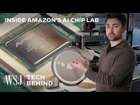
| AWS | Trainium 2 / Trn2 UltraServer (64 chips, 6 TB HBM, 83 PF FP8) | 4 × faster & 40 % cheaper than Trn1; up to trillion‑param training | AWS launch blog 03 Dec 2024 Amazon Web Services, Inc. |
| Microsoft | Maia 100 (5 nm, 4.8 Tb/s fabric, liquid‑cooled) | Built for Copilot & OpenAI workloads; open Triton kernels | Azure hardware deep‑dive Microsoft Azure |
| Meta | MTIA v2 dual‑die inference card | 5.5 × INT8 perf/W vs NVIDIA T4 at a fraction of cost | Meta technical post ServeTheHome |
Benchmark pulse: MLPerf Training v5.0 (June 2025) shows record submissions; Blackwell‑class and Gaudi 3 systems top most categories while AMD MI350 debuts strongly MLCommons.
4. AI goes bespoke — the cloud giants’ home‑grown chips
- Microsoft Maia 100 pairs 4.8 Tb/s Ethernet fabric with a 5 nm mega‑die and closed‑loop cooling to squeeze more accelerators per rack while meeting net‑zero goals Microsoft Azure.
- Google TPU v5p pods (released late 2024) remain Google’s internal training workhorse; TPU v6 is rumoured but not yet public.
- Meta MTIA v2 focuses on low‑cost inference at hyperscale, running ranking & Ads models with 3.5 × higher dense throughput Data Center Dynamics.
- Tesla Dojo D1/D2 wafer‑scale tiles feed FSD training and will ramp to > 500 MW of power draw at Gigafactory Texas over the next 18 months Wikipedia.
5. Edge & consumer “AI PCs”
| Silicon | NPU TOPS | Notable device class |
|---|---|---|
| Intel Lunar Lake | 45 TOPS on‑chip NPU; 100 + TOPS total with GPU | 2025 ultraportables Intel CDRD |
| AMD Ryzen AI 300 “Strix” | 50 TOPS NPU | Next‑gen ultrathin laptops (Copilot + spec) microchipusa.com |
| Qualcomm Snapdragon X Elite | 45 TOPS NPU | Windows‑on‑Arm notebooks Qualcomm |
| Apple M4 | 38 TOPS Neural Engine | iPad Pro (7th gen) & MacBook Air 2025 Apple |
These chips enable live translation, video up‑scaling and local LLMs without cloud latency.
6. Beyond electrons — photonic & analog frontiers
| Startup | Approach | 2025 milestone |
|---|---|---|
| Lightmatter | Silicon‑photonics “Envise” module performs matrix multiplies in light | Interposer shipping to customers in 2025; GlobalFoundries partner Lightmatter® |
| Celestial AI | Photonic Fabric optical chip‑to‑memory links | $250 m Series C1 led by Fidelity; $2.5 bn valuation Reuters |
| Mythic | Analog compute‑in‑memory (M2000 AMP) | 10 × energy drop vs digital for edge inference Highperformr |
| Groq | LPU (Language Processing Unit) for text inference | Public demos hit 500 tokens / s on Mixtral‑8×7B x.superex.com |
Photonics promises order‑of‑magnitude bandwidth gains, while analog promises watt‑level devices.
7. Memory, packaging & supply chain bottlenecks
- HBM4 (12‑ & 16‑high stacks, 24 Gb dies, 48 GB per package) moves into mass production H2 2025; SK hynix delivered first samples to NVIDIA, with Micron & Samsung racing to follow Tom’s Hardware.
- Advanced 2.5D/3D CoWoS capacity remains tight; TSMC admits supply will stay constrained into 2026 despite doubling lines AInvest.
- Jensen Huang notes NVIDIA is shifting to CoWoS‑L packaging to ease the crunch Reuters.
8. Energy & sustainability
Hyperscale “AI factories” are planned at 500 MW each in Italy, Canada and the UK to support multi‑exaflop clusters, driving urgency for renewable PPAs and liquid cooling EniData Center Dynamics. The EU AI Act now mandates energy‑transparency reporting for high‑risk AI systems, creating a regulatory push toward efficiency metrics like PUE < 1.2 and power‑use disclosure White & Case.
9. Policy & geopolitics
- U.S. export controls tightened again in Jan 2025; proposed chip‑level location‑tracking aims to curb GPU smuggling to China, though industry leaders warn it may accelerate domestic Chinese innovation Tom’s Hardware.
- China’s response is rapid investment in Huawei Ascend and Biren BR104 accelerators, but access to leading‑edge HBM and advanced‑node foundries remains limited by sanctions.
- The CHIPS & Science Act and Europe’s IPCEI programs continue to subsidise local packaging plants, while foundry giants expand in Arizona, Germany and Japan.
10. Five trends to watch next
- FP4 & FP6 everywhere: ultra‑low‑precision math (with error‑resilient training) is moving from research into production hardware.
- Chiplets + CXL 3.0: disaggregated GPU/CPU/Memory tiles stitched by coherent links for custom SKUs.
- Photonics at the board edge: early optical I/O reticles in 2025–26 will lift off‑package bandwidth 4–8 ×.
- AI‑native data‑centre design: rack‑scale cooling, 800 GbE fabrics and direct‑to‑chip liquid loops become standard.
- Edge sovereignty: countries plan “sovereign AI clusters” under EU AI Act to keep sensitive data local, spurring demand for on‑prem accelerators.
Glossary
- HBM High Bandwidth Memory, stacked DRAM soldered beside the GPU/ASIC.
- CoWoS Chip‑on‑Wafer‑on‑Substrate advanced packaging from TSMC.
- TOPS Tera (10¹²) Operations per Second, typical NPU metric.
- MLPerf Industry‑standard benchmark suite maintained by MLCommons.
Compiled 7 Aug 2025. All hyperlinks correspond to the cited public sources.


")