Table of Contents
- Executive Summary: Key Market Drivers and 2025 Outlook
- Current State of Monolayer Graphene Synthesis: Methods and Leading Players
- Breakthroughs in Chemical Vapor Deposition (CVD) and Emerging Alternatives
- Major Industry Collaborations and R&D Initiatives (2024–2025)
- Supply Chain and Scale-Up: Overcoming Production Bottlenecks
- Cost Analysis: Price Trends and Commercialization Challenges
- Key Applications: Electronics, Energy Storage, and Beyond
- Competitive Landscape: Profiles of Top Manufacturers and Innovators
- Market Forecasts: Growth Projections Through 2030
- Future Outlook: Next-Gen Technologies and Strategic Opportunities
- Sources & References
Executive Summary: Key Market Drivers and 2025 Outlook
Monolayer graphene synthesis technologies are entering a pivotal phase in 2025, driven by increasing industrial demand for high-quality, scalable, and cost-effective production methods. The sector’s main growth engine is the expanding application base, particularly in advanced electronics, energy storage, and next-generation composite materials. Key market drivers include the pursuit of wafer-scale uniformity, integration with semiconductor manufacturing, and the demand for sustainable, reproducible synthesis processes.
Chemical vapor deposition (CVD) remains the dominant method for producing high-quality monolayer graphene at commercial scales. Major industry participants such as Graphenea and Grolltex are scaling up CVD-based manufacturing lines to meet requirements for electronic, sensing, and photonics applications. In 2025, these companies are focusing on process innovations to enhance layer uniformity and reduce production costs. For instance, Graphenea has implemented roll-to-roll CVD systems designed to supply continuous films for flexible electronics, while Grolltex is emphasizing single-layer purity and CMOS compatibility for electronics integration.
Beyond CVD, alternative synthesis approaches are gaining traction. Plasma-enhanced CVD and molecular beam epitaxy are being evaluated for their ability to lower synthesis temperatures and improve control over layer properties. 2D Carbon Tech is advancing plasma-based techniques, reporting improved throughput and substrate versatility targeting display and battery manufacturers. Additionally, scalable epitaxial growth on silicon carbide is being pursued by Epigrafen for high-frequency electronics markets.
Market momentum is further accelerated by strategic partnerships and public-private initiatives. Organizations such as the Graphene Flagship are coordinating joint efforts between industry and academia to standardize synthesis protocols and ensure quality assurance. These collaborations are facilitating the transition from laboratory-scale breakthroughs to robust industrial processes.
Looking ahead through 2025 and into the next several years, the outlook for monolayer graphene synthesis technologies is optimistic. Key trends include the commercialization of large-area, defect-free graphene films, integration with semiconductor processes, and increased adoption in mass-market applications such as sensors and flexible displays. Continued investment in process scalability and quality control, supported by an expanding ecosystem of suppliers and end-users, is expected to underpin robust market growth and technological diversification.
Current State of Monolayer Graphene Synthesis: Methods and Leading Players
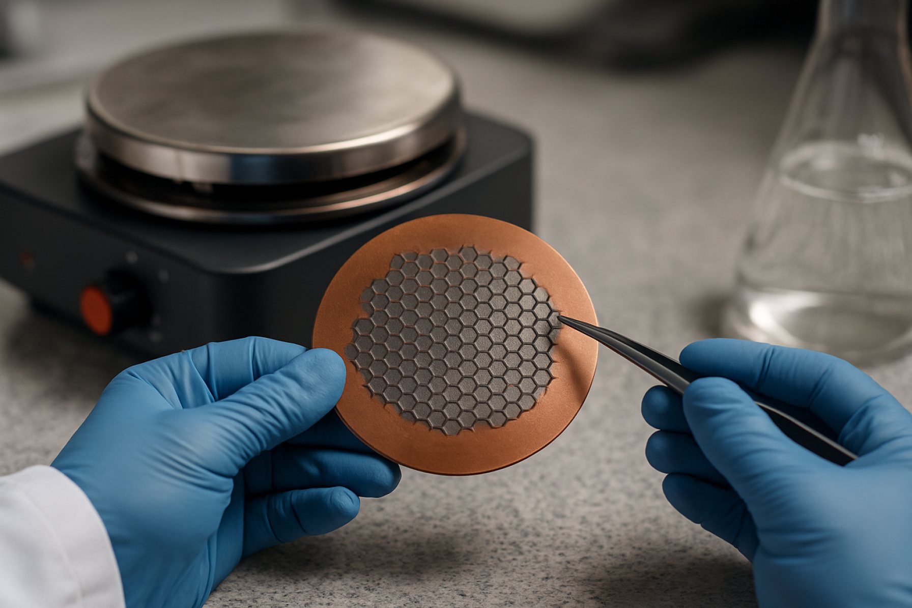
As of 2025, monolayer graphene synthesis technologies have advanced significantly, with chemical vapor deposition (CVD) emerging as the most reliable and scalable method for producing high-quality monolayer graphene on industrial scales. CVD processes typically use substrates such as copper or nickel, allowing the growth of large-area graphene films with controlled thickness and crystallinity. Leading players in this sector have reported continuous improvements in throughput, uniformity, and transfer techniques to meet the demands of electronics, photonics, and advanced materials industries.
Among the notable companies, Graphenea has developed proprietary CVD growth processes that deliver monolayer graphene films with high carrier mobility and low defect densities, addressing critical requirements for semiconductor and sensor applications. Their 2024 product lines feature wafer-scale monolayer graphene on a variety of substrates, with ongoing process optimization targeting even larger formats and improved transfer yields.
Another technology leader, 2D Carbon (Changzhou) Tech Inc., has focused on roll-to-roll CVD graphene production, enabling meter-scale continuous synthesis suitable for flexible electronics and transparent conductive films. Their advancements in reactor design and substrate handling are setting new benchmarks for production speed and cost efficiency in 2025.
Alternative synthesis methods such as plasma-enhanced CVD (PECVD), molecular beam epitaxy (MBE), and epitaxial growth on silicon carbide (SiC) continue to be refined for specific high-performance or niche applications. Graphene Platform Corporation offers monolayer graphene produced via both CVD and MBE for research and prototyping, highlighting the versatility of methods available depending on end-use requirements.
Vertically integrated companies like Directa Plus are investing in hybrid technologies that combine CVD with post-synthesis treatments to tailor surface chemistry and electronic properties, further expanding the application space for monolayer graphene. Additionally, organizations such as the Graphene Flagship are supporting collaborative pilot lines and industrial-scale demonstrations to accelerate the commercialization timeline.
Looking ahead, the immediate outlook includes further scaling of CVD reactors, automation of graphene transfer processes, and integration into semiconductor wafers, with several manufacturers announcing plans for 12-inch wafer monolayer graphene production lines by 2026. Collectively, these efforts are poised to bridge the gap between laboratory-scale synthesis and mass-market adoption, positioning monolayer graphene as a foundational material for next-generation technologies.
Breakthroughs in Chemical Vapor Deposition (CVD) and Emerging Alternatives
The landscape of monolayer graphene synthesis is experiencing significant advancements in 2025, with Chemical Vapor Deposition (CVD) maintaining its position as the dominant industrial-scale method while alternative technologies rapidly mature. The CVD process, particularly on copper substrates, continues to deliver high-quality, large-area monolayer graphene suitable for electronics, sensors, and advanced composites. Leading industrial players such as Graphenea and Graphene Technologies have expanded their production lines in the past year, leveraging optimized low-pressure and atmospheric pressure CVD processes that enable monolayer coverage across 300 mm wafers, a critical scale for semiconductor integration.
Recent breakthroughs focus on process control, substrate engineering, and post-growth transfer methods. For example, Graphenea has reported improvements in continuous roll-to-roll CVD that enhance uniformity and reduce contamination during the transfer process, addressing a longstanding bottleneck for device-grade graphene. Meanwhile, 2D Carbon Tech has demonstrated copper foil engineering that minimizes grain boundaries, resulting in higher carrier mobility and lower defect densities in monolayer films.
Emerging alternatives to CVD are also showing promise for both scalability and cost-effectiveness. Plasma-enhanced CVD (PECVD) is being commercialized by companies such as Directa Plus, allowing for lower-temperature synthesis compatible with flexible substrates, opening up applications in wearable electronics and transparent conductors. Furthermore, Metal-Organic CVD (MOCVD) and remote epitaxial growth are moving from pilot lines to early production, as exemplified by Grolltex, which has recently scaled up its single-layer graphene output to support energy storage and biosensor markets.
Looking forward, the sector anticipates further integration of artificial intelligence and machine learning to optimize process parameters in real-time, as piloted by Graphenea’s smart manufacturing initiatives. The next few years are expected to see the first commercial devices featuring monolayer CVD graphene in displays, photonics, and microelectromechanical systems (MEMS), driven by improvements in reproducibility and cost reduction. With ongoing investment and collaboration between technology providers and end-users, monolayer graphene synthesis technologies are poised to transition from specialized research materials to foundational components in mainstream electronics and advanced materials markets.
Major Industry Collaborations and R&D Initiatives (2024–2025)
The period from 2024 to 2025 is witnessing significant industry collaborations and research & development (R&D) initiatives focused on advancing monolayer graphene synthesis technologies. Key players in the sector are investing in scalable, high-quality production methods, with an emphasis on chemical vapor deposition (CVD) and novel hybrid approaches.
A major milestone was reached in late 2024 when Graphenea, a leading European graphene producer, announced a collaborative project with several academic partners to scale up roll-to-roll CVD synthesis of monolayer graphene on copper foils. This initiative aims to optimize both throughput and uniformity, targeting electronics and sensor markets where wafer-scale monolayer consistency is critical. Similarly, AMG Graphite has expanded its R&D collaboration with technology institutes in Germany, focusing on transferring lab-scale CVD methods to pilot-scale production lines, with results expected in early 2025.
In Asia, Nippon Graphite Industries, Ltd. and Mitsubishi Chemical Group have announced joint research targeting improved catalyst substrates for CVD growth. Their 2025 roadmap includes the deployment of proprietary substrate treatments designed to enhance monolayer domain size and reduce defect density, a breakthrough for next-generation optoelectronic and quantum devices.
North American players are also taking bold steps. Universal Matter Inc. is partnering with Canadian and U.S. universities to commercialize its ‘flash graphene’ process, which reportedly delivers monolayer graphene at lower energy costs. The company’s pilot plant, scheduled for completion in 2025, will allow direct benchmarking against conventional CVD processes.
Furthermore, cross-industry alliances are forming to address downstream integration challenges. Samsung Electronics is collaborating with materials suppliers and semiconductor foundries to integrate monolayer graphene into transistor channels, as part of its 2D materials R&D program. This joint effort leverages advances in CVD synthesis and transfer technologies, with prototype CMOS devices anticipated by late 2025.
Overall, the next few years are expected to bring accelerated progress toward industrial-scale, defect-free monolayer graphene, driven by multi-partner consortia and an expanding R&D ecosystem. These efforts are laying the groundwork for graphene’s adoption in electronics, photonics, and advanced composites.
Supply Chain and Scale-Up: Overcoming Production Bottlenecks
The scale-up of monolayer graphene synthesis technologies is a central challenge for the commercialization of graphene-based applications in 2025 and the near-term future. Chemical vapor deposition (CVD) on copper remains the predominant method for producing large-area, high-quality monolayer graphene. Companies such as Graphenea and 2D Carbon (Changzhou) Tech have established CVD production lines capable of supplying wafers and roll-to-roll products, but the bottleneck persists in consistent wafer-scale uniformity and the minimization of defects during transfer and integration.
Key supply chain challenges stem from substrate quality, reactor scalability, and the reproducibility of monolayer growth. The transition from lab-scale (centimeter-scale) to commercial wafer sizes (upwards of 200 mm and beyond) has required advanced reactor engineering and process monitoring. 2D Carbon (Changzhou) Tech has reported continuous roll-to-roll production, enabling meter-scale graphene films, yet maintaining single-layer integrity over large areas remains non-trivial. Similarly, Graphenea offers high-quality monolayer graphene on copper foils and SiO2/Si wafers, but production capacity is still measured in thousands of wafers per year, indicating a gap between demand forecasts and current output.
Emerging approaches aim to address these scale-up limitations. Direct growth of graphene on dielectric substrates—pioneered by organizations such as IBM—could eliminate transfer processes, reducing contamination and improving device yields. Additionally, companies like Advanced Graphene Products are developing proprietary CVD reactor designs targeting higher throughput and improved uniformity for industrial clients. Automation and in-line metrology are being integrated to enhance reproducibility and traceability throughout the supply chain.
Looking forward, the next few years are likely to see progress in both production throughput and quality, driven by investments from electronics, energy storage, and composite materials sectors. Strategic partnerships between equipment manufacturers, materials suppliers, and end-users are accelerating the optimization of synthesis parameters and downstream integration techniques. As regulatory bodies such as Graphene Flagship and international standards organizations continue to define characterization benchmarks, the industry’s ability to guarantee consistent monolayer graphene supply is expected to improve. Nonetheless, closing the gap between pilot and full-scale manufacturing will require ongoing innovation in reactor design, substrate engineering, and process control.
Cost Analysis: Price Trends and Commercialization Challenges
Monolayer graphene synthesis technologies have witnessed significant shifts in pricing and commercialization strategies as the industry matures toward 2025. The cost of monolayer graphene remains a critical factor influencing its widespread adoption in electronics, energy storage, and advanced materials. Chemical vapor deposition (CVD) dominates commercial-scale production, with key players such as Graphenea and 2D Carbon (Changzhou) Tech Inc. leveraging scalable CVD processes to deliver high-quality, large-area monolayer graphene films. Despite technological gains, the price for monolayer graphene produced via CVD currently ranges from several tens to hundreds of dollars per square centimeter, depending on substrate, purity, and order scale.
Efforts to reduce production costs have centered on optimizing catalyst substrates, recycling copper foils, and enhancing process throughput. For example, Graphenea has reported incremental improvements in roll-to-roll CVD, aiming for continuous production and reduced labor costs. Similarly, Directa Plus S.p.A. has invested in modular reactor designs and post-synthesis purification steps to improve yield and consistency, which are essential for commercial viability.
However, several commercialization challenges persist. The primary bottleneck remains the synthesis of uniform, defect-free monolayer graphene on a large scale. Even minor variations in film thickness or domain boundaries can affect electronic and mechanical properties, hampering device integration. Furthermore, substrate transfer processes—necessary for most end-use applications—add complexity and cost. AMG Advanced Metallurgical Group N.V. and Graphene Square Inc. are actively developing automated transfer and patterning techniques to mitigate these issues, but industrial-scale reliability is still a near-term goal.
From a market perspective, price declines are anticipated over the next few years as production efficiency increases and demand from sectors such as flexible electronics and biosensors scales up. Companies like Graphenea expect gradual cost reduction as their facilities move towards higher automation and greater production volumes. Nevertheless, the price gap between monolayer and multilayer (or reduced graphene oxide) graphene remains wide, with multilayer products often available at a fraction of the cost, thus constraining monolayer uptake in price-sensitive applications.
In summary, while the path to cost-competitive, large-area monolayer graphene remains challenging, ongoing process innovations and scaling investments by leading manufacturers are likely to bring incremental price drops and improved material quality within the next few years, paving the way for broader commercial adoption.
Key Applications: Electronics, Energy Storage, and Beyond
The commercial and research-driven demand for monolayer graphene continues to fuel innovation in synthesis technologies as of 2025. High-quality, large-area monolayer graphene is essential for next-generation electronics, advanced energy storage, and emerging applications such as biosensors and photonic devices. Among the scalable techniques, chemical vapor deposition (CVD) remains the industry standard, with incremental improvements targeting uniformity, yield, and substrate compatibility.
Recent advancements by leading suppliers focus on optimizing CVD processes to minimize defects and increase wafer sizes. Graphenea, for instance, offers monolayer CVD graphene on copper and insulating substrates, with sheet sizes now reaching up to 300 mm, supporting integration with semiconductor fabs. Similarly, 2D Carbon (Changzhou) Tech Inc. has automated their roll-to-roll CVD lines, pushing throughput and consistency for electronics and battery manufacturers.
In 2025, alternatives to copper substrates are gaining traction to enable direct transfer and device integration. Samsung Electronics has demonstrated CVD growth of monolayer graphene directly on insulating substrates, reducing the contamination and damage associated with traditional transfer methods—a critical step for commercial electronics applications.
Plasma-enhanced CVD (PECVD) and low-temperature CVD are being refined to enable synthesis on flexible and temperature-sensitive substrates, expanding use in flexible electronics and wearable devices. Companies such as Grolltex are commercializing graphene grown at lower temperatures, aiming to serve the burgeoning wearable sensor market.
Beyond CVD, epitaxial growth on silicon carbide (SiC) is being explored for its potential to yield high-mobility monolayer graphene suitable for high-frequency electronics. Graphensic AB continues to supply epitaxial graphene wafers, targeting researchers and specialized device manufacturers.
Looking ahead, industrial players anticipate further scale-up of continuous production systems and digital process control, with efforts to reduce costs and environmental impact. The next few years are likely to see more robust supply chains and quality standards, driven by collaboration between synthesis technology providers and end-users. Collectively, these developments are expected to accelerate the adoption of monolayer graphene in advanced electronics, energy storage, and beyond.
Competitive Landscape: Profiles of Top Manufacturers and Innovators
The competitive landscape for monolayer graphene synthesis technologies in 2025 is characterized by a consolidation of key industrial players, alongside a vibrant ecosystem of innovators pushing the boundaries of scalable and high-quality production. Companies at the forefront are leveraging advanced chemical vapor deposition (CVD), plasma-enhanced CVD, and novel substrate engineering to achieve consistent, wafer-scale monolayer graphene with minimal defects and high carrier mobility.
A leader in the field, Graphenea, continues to expand its offerings in CVD-grown monolayer graphene, targeting both industrial partners and research institutions. Their ability to deliver high-uniformity films on substrates up to 8 inches positions them as a preferred supplier for electronics and sensor applications. Graphenea’s focus on process standardization has led to improved yield rates and reproducibility, addressing a long-standing challenge in graphene commercialization.
In Asia, SixCarbon Technology has made substantial advances in scaling up its roll-to-roll CVD methods, reportedly achieving continuous production of monolayer graphene films exceeding 1 meter in length. This capability is crucial for flexible electronics and transparent conductive films, areas where large-area uniformity is essential. Their proprietary process optimization has reduced defect density and improved electronic performance, contributing to the acceleration of commercialization efforts.
In the United States, Grolltex is notable for its patented single-layer graphene production directly on copper foils, which are subsequently transferred to various substrates. Their focus on electronic-grade material and automated transfer processes aims to serve the growing demand from semiconductor and photonics industries. By early 2025, Grolltex has expanded its production capacity and formed strategic partnerships with device manufacturers to integrate monolayer graphene into next-generation components.
Collaborative research and industry consortia also play a pivotal role. The Graphene Flagship consortium continues to drive joint projects among European industry leaders and academic groups, accelerating the translation of monolayer graphene synthesis breakthroughs into commercial products. Their pilot lines and demonstrator projects focus on quality control, upscaling, and new application development.
Looking ahead, the next few years are expected to witness further improvements in cost-efficiency, process scalability, and integration compatibility, especially as demand rises from sectors such as flexible displays, advanced sensors, and energy storage. The competitive advantage will likely shift toward companies that can demonstrate robust supply chains, consistent product quality, and the ability to customize graphene properties for specific end-use cases.
Market Forecasts: Growth Projections Through 2030
The global market for monolayer graphene synthesis technologies is poised for robust growth through 2030, underpinned by rising demand across sectors such as electronics, energy storage, and advanced coatings. As of 2025, advancements in chemical vapor deposition (CVD) and roll-to-roll (R2R) processes are enabling higher throughput and improved quality, addressing previous scalability and uniformity bottlenecks.
Key industry players have expanded their production capacities in response to increasing commercial orders. For example, Graphenea continues to enhance its CVD monolayer graphene lines, targeting sectors from sensors to quantum devices. Similarly, Directa Plus has invested in scalable production methods, focusing on environmentally friendly synthesis and integration into industrial applications.
Ongoing improvements in process control and substrate compatibility are expected to drive down production costs, making monolayer graphene more accessible for mass-market applications. Grolltex reports progress in its R2R graphene synthesis, aiming to deliver wafer-scale monolayer films for electronics and photonics. These capabilities support projections that the market for high-quality monolayer graphene will grow at a double-digit CAGR through 2030, as new applications in flexible displays, batteries, and filtration materials reach commercialization.
Public-private collaborations and increased funding for pilot-scale facilities are accelerating technology transfer from laboratory to industry. For instance, Graphene Flagship, a major pan-European initiative, is actively supporting the scale-up of synthesis technologies and the establishment of standardized quality metrics, which is vital for widespread adoption.
Looking ahead, the outlook for monolayer graphene synthesis technologies remains highly positive. The next few years will likely see further breakthroughs in continuous manufacturing, defect minimization, and integration with semiconductor fabrication. By 2030, the convergence of mature synthesis platforms, expanded end-use cases, and supportive regulatory environments is expected to propel the global market to multi-billion-dollar valuations, with Asia, Europe, and North America as key growth regions.
Future Outlook: Next-Gen Technologies and Strategic Opportunities
Monolayer graphene synthesis technologies are approaching a pivotal phase in 2025, with a clear trend toward scalable, high-quality, and cost-effective production methods. Chemical vapor deposition (CVD) remains the dominant commercial approach, but recent developments point to significant improvements in both throughput and quality control. Companies like Graphenea and 2D Carbon (Changzhou) Tech have implemented CVD processes that routinely yield monolayer films with uniformity over 300 mm wafers, addressing a longstanding scalability challenge. In 2024, Graphenea announced upgrades to its continuous roll-to-roll CVD lines, projecting reductions in defect density and improved reproducibility for electronics and sensor markets.
Direct growth on dielectric substrates—bypassing the need for metal catalysts and transfer steps—has gained momentum as a next-generation approach. AMSC Insulators and Oxford Instruments are actively developing plasma-enhanced CVD (PECVD) and remote epitaxy solutions, which promise lower contamination and integration with silicon CMOS workflows. Early 2025 pilot results indicate that these methods can achieve monolayer coverage with mobility values approaching those of exfoliated graphene, a key metric for device-grade material.
Other promising methods include molecular beam epitaxy (MBE), which is being refined for industrial viability by Siemens in collaboration with academic partners, and scalable liquid-phase exfoliation from companies such as Directa Plus, though the latter currently yields multilayer dominant dispersions. Meanwhile, NovaCentrix is piloting novel laser-induced graphene formation on flexible substrates, targeting rapid prototyping and additive manufacturing applications.
From a strategic perspective, the next few years will see increased co-development between graphene producers and end-users in semiconductors, photonics, and energy storage. “On-site” or “tool-integrated” graphene growth, as being explored by Lam Research, could enable direct device fabrication—eliminating costly transfer processes. Industry consortia, such as the Graphene Flagship, are also funding pilot lines to bridge the gap between lab-scale innovation and reliable wafer-scale supply.
Overall, the outlook for monolayer graphene synthesis is robust, with pilot-scale breakthroughs in 2025 expected to translate into commercial adoption by 2027–2028, particularly for applications demanding electronic-grade, large-area films.


